Inorganic Trace Analytics, mainly in Micrograde and SolargradePolysilicon- and Silicon Products and its Upstream and Downstream Manufacturing Products
Since the 1950s, silicon, the second most abundant element, has been widely used to produce integrated circuits. Silicon is not found free in the nature, but it occurs as oxide or silicate.Crystalline, pure silicon has a grayish color and an easily formed and tightly adherent oxide; is quite inert to most acids but hydrofluoric acid (HF) readily attacks its oxide form. Silicon´s oxidation properties make it the primary semiconductor material for the integrated circuit manufacturing and for the solar cell fabrication. Single silicon crystal has low conductivity; to obtain the electrical characteristics desired it is necessary to introduce specific dopant atoms into the silicon. Oxidation and diffusion are the basic processes mainly in semiconductor manufacturing but also in solar cell fabrication these processes keep an important role. Due to increased electronic density, finer circuit patterns and the production of more efficient solar cells the performances of these semiconductors and solar wafers are greatly influenced by the mobility of metallic contaminants within the devices. The extent of cleanliness required in processing has therefore increased. Wet processing is mostly one principal step of the silicon micromachining process. Since aqueous etchings and reagents come into direct contact with the silicon material, quality-purity tests of the contaminants in these chemicals become more and more important. The drive towards the reduction of these contaminants has led to the need of higher sensitivity analytical methods to be used for the cleanliness evaluation. The importance of thoroughly cleaning silicon surfaces prior to any temperature process, oxidation or diffusion, has long been recognized. Poorly prepared silicon wafer surfaces can give rise to many local regions of imperfections. The purity of wafer surfaces is an essential requisite for the successful fabrication of very large scale integrated (VLSI) and ultra large scale integrated (ULSI) silicon circuits. Metal contaminants such as Fe, Ni, Cu and Zn, are detrimental for present semiconductor surfaces and nowadays even for solargrade material, because they spread and diffuse into the silicon bulk especially during high-temperature processing and reduce the lifetime of the carrier while increasing dark and leakage current. Dopant elements such as B, P, Al, As can shift the devices operating characteristics.However, autodoping impurities and particulate contaminations of any kind of silicon surface can have serious impact on the device performance and yields.According to the more stringent requirements for increased device performance and an improved process yield, the impurity level for metals on silicon surfaces will be driven to more and more lower levels. For the development of techniques to avoid contamination and of processes to generate very clean surfaces and bulk, highly sensitive surface analytical techniques and special designed methods have become critically important, even in the most upstream processes of polysilicon production.
Our research interest lies in the analytical method development, Quality and data evaluation of various Polysilicon-Production steps such as TCS/STC-Distillation, Tankfarm management concept and Solid Post-processing steps. The most important steps here are:
Surface-, Subsurface- and Bulk analysis of Polysilicon Chunks by ICP-MS/INAA
(Method Development, Benchmarking, Correlation, Interferences, Sample Preparation Methods, Standardization, Limit of Detection, Sensitivity, UPW Analysis)
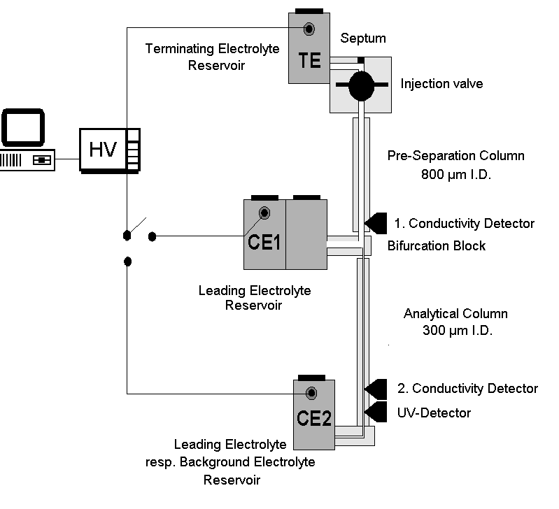
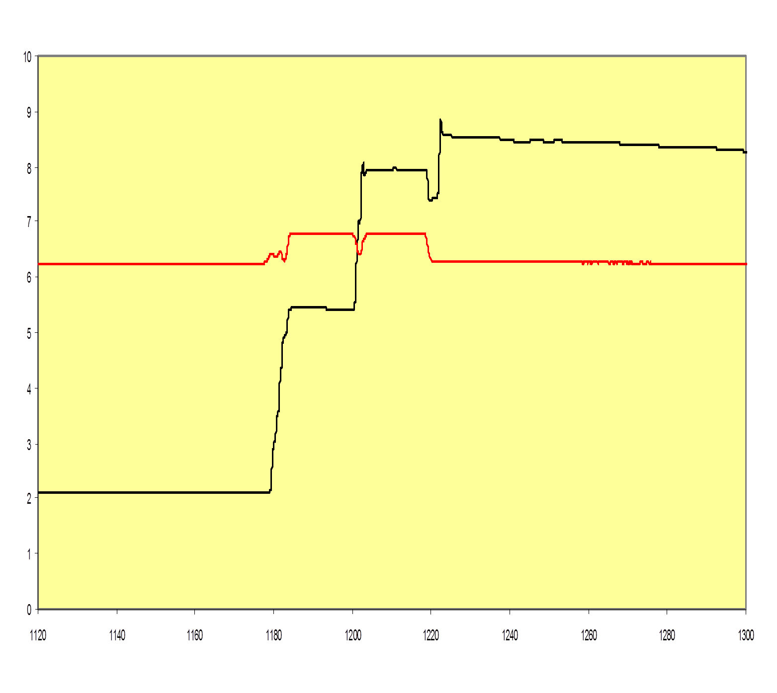
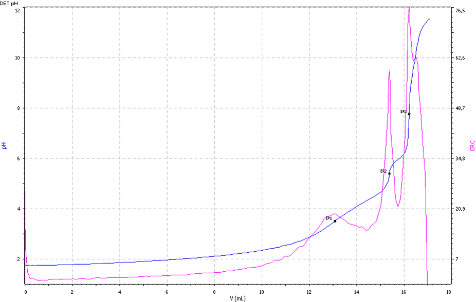
Method Development and Routine Analysis of Etching Solutions by ICP-OES and Online Titration
Method Development and Routine Analysis of TCS/STC Samples by ICP-OES and ICP-MS for Metals and Boron/Phosphorous in Different Production Steps (distillation, tankfarm)
Method Development / Routine Analysis of MG-Silicon Samples by ICP-OES and GD-MS, Correlation, Benchmarking, Supplier Evaluation
Boron-, Phosphorous- and Carbon Analysis by Test Deposition and in Drilled Polysamples by LT-FTIR on FZ-Mono and Carbonanalysis on Polysilicon (Sample-preparation, Depth-profiling)
µ-PCD Sample Preparation and its influence on the final results
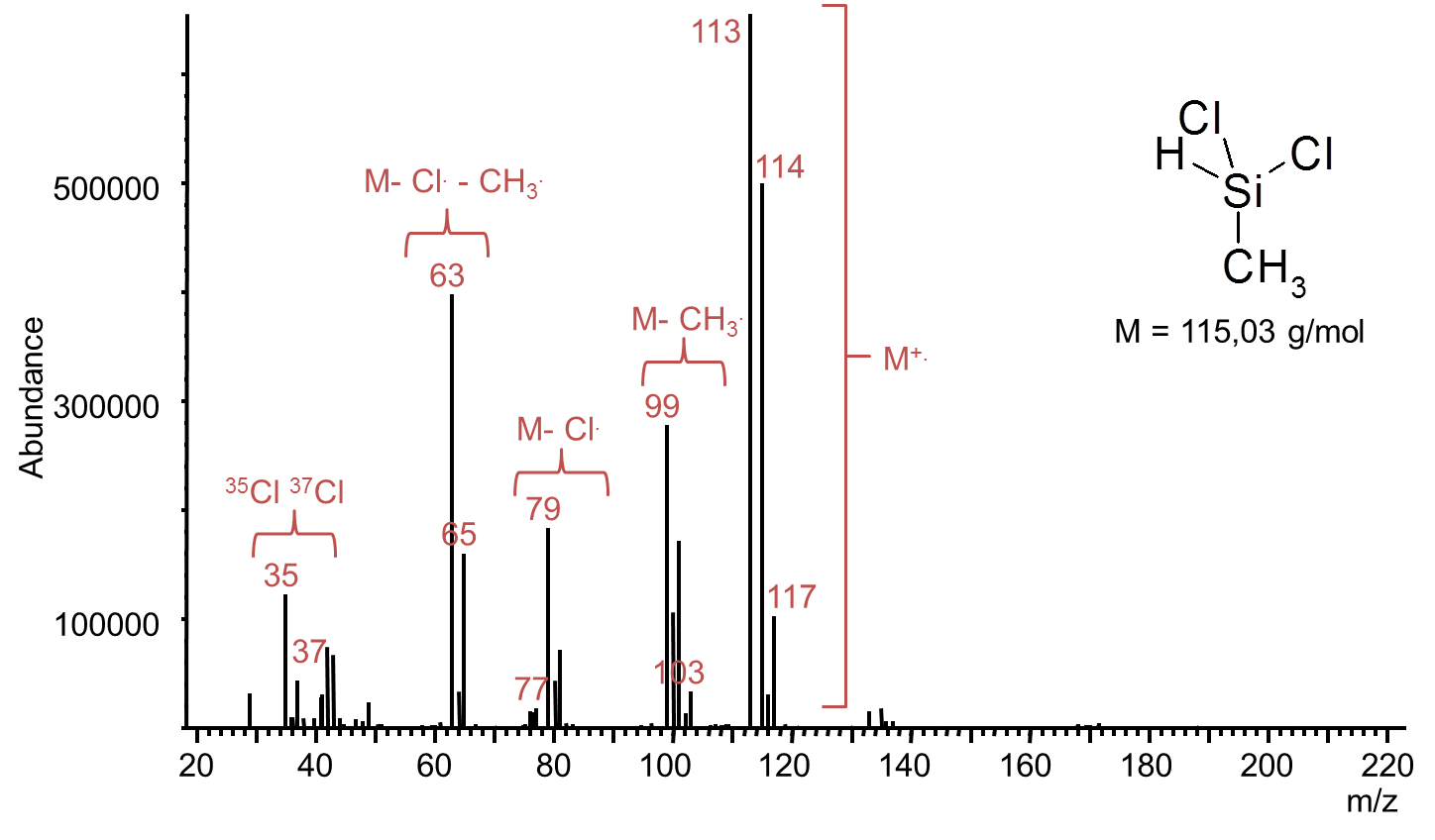
GC and GC-MS Analysis for TCS / STC / DCS / MDCS, Offline and Online
Sampling for GC Analysis, Process-GC
Data Analysis / Contamination Sources / Implementation of Quality Meetings with responsible production people
Basic Engineering and Detailed Engineering of Polysilicon Laboratories
Supplier Evaluation / Procurement of Analytical Equipment and Preparation Equipment
Chunk and Granular Etching in Production, Evaluation of Different Technologies Characterization by Online Titration
Development of an Analytical Preparation Equipment for Granular Polysilicon, Analytical Method Development
Evaluation / Benchmark of Different Granular Forms